Scanning electron microscopy and EPMA
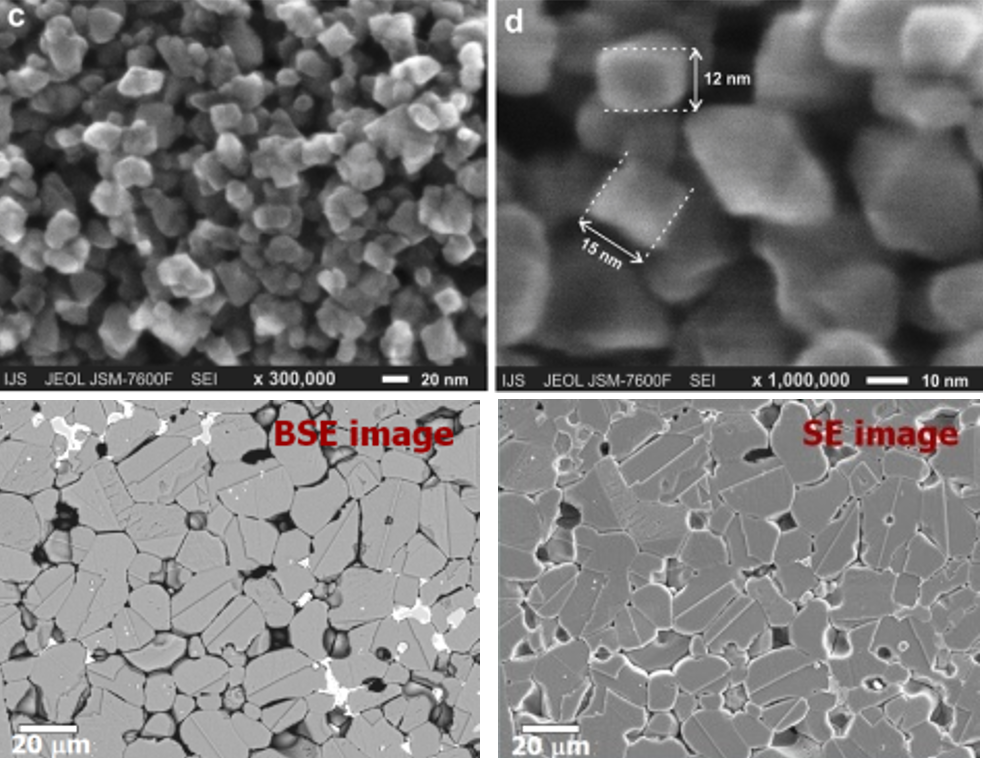
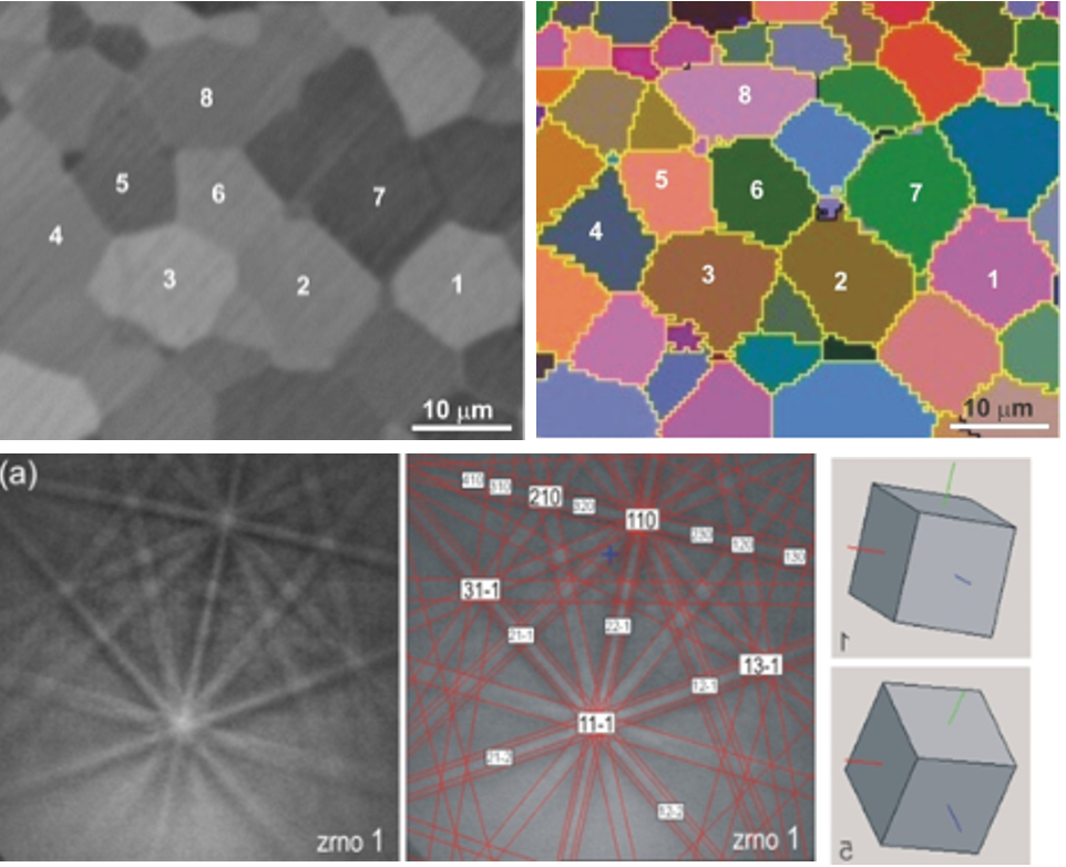
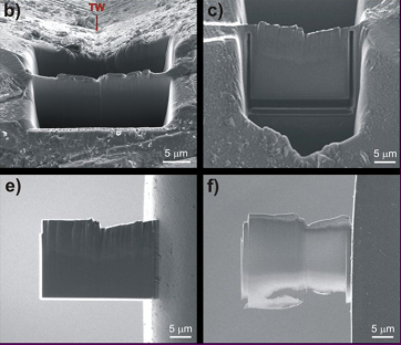
Scanning electron microscopy (SEM) readily provides images of the surface morphology of investigated materials down to nm level. Combined with spectroscopy techniques it additionally enables determination of the chemical composition of investigated materials in bulk and layered structures with analytical spatial resolution in micrometre range. The group has vast knowledge in SEM (SE, BSE, ADF) imaging as well as in semi-quantitative and quantitative EDS and WDS analysis using large set of standard/reference materials. The crystallographic studies of materials, i.e. texture determination, are obtained by the EBSD. E-lithography is also available on the FEG-SEM.

Contact:
Transmission electron microscopy
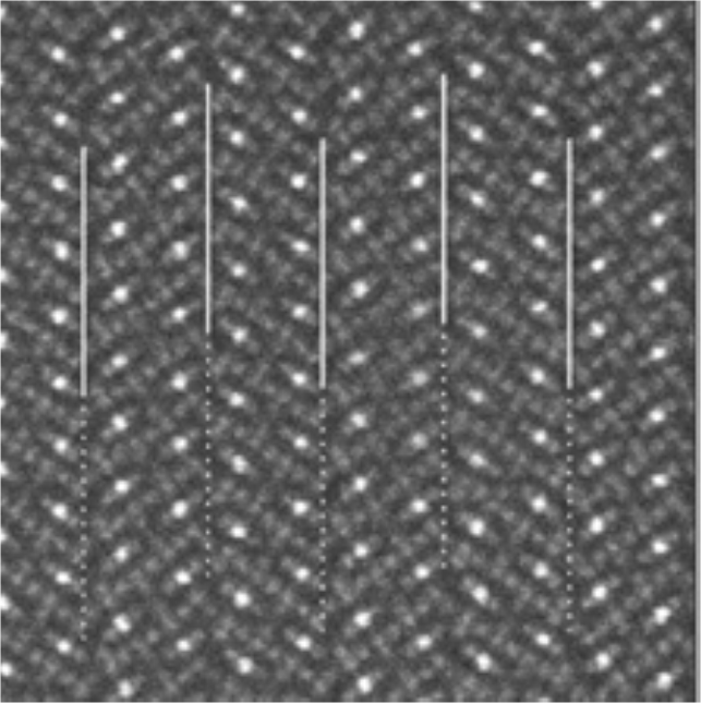
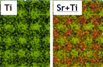
Transmission electron microscopy (TEM) and scanning transmission electron microscopy (STEM) techniques combined with spectroscopic methods (EDS, EELS) readily provide structural and chemical information of materials on nano and atomic scale. While electron diffraction techniques (SAD, CBED, precession technique) provide information on the structure of crystalline nanostructures (grains, precipitates, etc.), HRTEM imaging with image simulations yield structural models of interfaces and planar faults. STEM ADF, HAADF and ABF provide atom resolved chemical information based on the measured intensities of individual atom columns. Chemical information can be further obtained by EDS and EELS (atom resolved mappings, line profiles, 2D valence state distribution, plasmonic studies, etc.). The research groups has access to the state-of-art (S)TEM equipment, i.e. Cs corrected STEM, and a long term collaboration with the partners within the ESTEEM and ESTEEM2 consortium.

Contact:
In situ electron microscopy
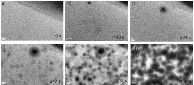
Significant advances in the development of novel functional nanomaterials can be achieved by using suitable microscopy methods that allow in situ dynamic investigations of nanomaterials in their native environments at the highest spatial resolution. That includes nanoscale dynamic studies of nucleation and growth of nanomaterials as a function of temperature (in-situ heating/cooling). To bridge the gap between conventional (high-vacuum) and in-situ liquid TEM we have recently implemented an interdisciplinary research platform for dynamic TEM studies in liquid environments that are overcoming the static limitations of conventional analysis techniques. This ground-braking approach opens wide range of possibilities in high-resolution in situ dynamic studies where case-by-case specialized experiments can be performed by proper redesign of liquid chambers, allowing to perform direct nucleation and growth studies of nanoparticles either from solutions or during the electrodeposition, at the nanoscale and in real time.
Contact:
Modelling of technologically important properties
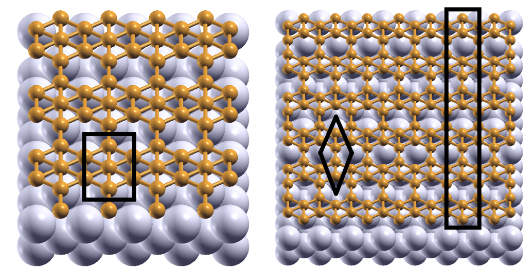
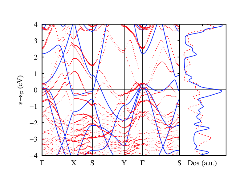
Design of novel materials with well-defined target properties is no more based just on a trial-and-error approach but it is ever more oriented towards understanding the background mechanisms responsible for the observed behavior. Fundamentally all processes in materials originate from interactions between the electrons forming the matter, which can be explained in terms of quantum mechanics. Therefore the complete understanding of the relation between the electronic structure and the results of various experiments, from the X-ray scattering, electron-microscope imaging, the measurements of mechanic, thermal, electric, magnetic and other properties, is of great importance. At the Department for Nanostructured materials of Jožef Stefan Institute we combine experimental activities with ab-initio modelling within the framework of the density-functional theory. This is the state-of-the-art method to simulate the ground-state crystal structures, magnetic ordering, elasticity, response to various external fields etc. without adjusting any phenomenological parameters,, just by applying the electron configuration of the included atoms and starting atomic positions.
The results of such calculations can serve either as a prediction or as an interpretation of experimental findings.