

Contact person: Sašo Šturm, e-mail: saso.sturm@ijs.si
Contact person: Sašo Šturm, e-mail: saso.sturm@ijs.si
The Advanced Electron Microscopy Group develops and implements cutting-edge electron microscopy techniques for materials characterisation.
Our approach creates a seamless integration between material synthesis, atomic-scale structural and chemical characterisation, and the resulting physical properties, supported by atomic-level modelling based on Density-Functional theory (DFT). We employ diverse Electron Microscopy (EM) techniques for advanced nanomaterial characterisation, focusing on extracting detailed information from material’s interfaces. Recently, we have focused on 4D Scanning Transmission Electron Microscopy (STEM/4D-STEM) and electron ptychography to reconstruct the electron exit wave, coupled with computational microscopy for high-data, high-speed processing and smart automatisation of microscopy procedures. In experimental microscopy, we employ in-situ TEM techniques to study materials in their natural environments and under dynamic conditions, in-opreando. Additionally, we continuously innovate specimen preparation routines using focused ion-beam technology to support advanced TEM analysis.
We studied RE-Au-Si systems, which are 1/1 Tsai-type quasicrystalline approximants with cluster center decoration, which can be distorted tetrahedrons, rare earth atoms or intermediate clusters of randomly distributed distorted tetrahedrons and rare earth atoms. We showed that by correlating line intensity profiles extracted from experimentally obtained high-angle annular dark field STEM (HAADF-STEM) images with line intensity profiles extracted from corresponding simulated images, it is possible to determine which kind of cluster centre decoration is present in studied materials. In particular, we found that due to probe channelling in scanning direction coinciding with the (Figure 20) crystallographic plane across the center of the cluster, the presence of distorted tetrahedron results in intensity broadening while rare-earth atom at the center results in sharp intensity. The results of this study were published in the Israel Journal of Chemistry (https://doi.org/10.1002/ijch.202300117).

Figure 20: Combining scanning transmission electron microscopy images and their simulations with X-ray diffraction allows (https://doi.org/10.1002/ijch.202300117)
Recent development of liquid-cell TEM holders allows for in-situ studying of materials reactions. Such specialised holders contain liquid cells that can withhold liquid in a confined environment, facilitating the imaging and spectroscopy of samples in reaction media. One of the most studied chemical processes in liquid TEM is related to studies of nucleation, growth, and dissolution processes of nanoparticles and nanostructures. Moreover, combining the capabilities of liquid-cell TEM holders with microsize electrodes printed on a chip, i.e. the in-situ electrochemical liquid transmission electron microscopy (EC-LTEM), enables us to study dynamic phenomena during electrochemical reactions at high spatial and temporal resolution.
This is also the subject of a SLO-FWO joint project where we use the EC-LTEM to investigate the dynamics of the electrochemical deposition and dissolution of metallic nanoparticles (NPs) such as Au, Ag, Pt, and Pd by directly visualising them during the process. In our recent study, we tackled the dissolution process of Au NPs under electrochemical biasing. In-situ EC-LTEM observations showed that upon potentiostatic polarisation, Au NPs dissolve at different stages, revealing a core-shell structure during the dissolution. The shell, which is more resistant, leads to a delayed, particle-by-particle dissolution process once broken down. This phenomenon can be seen in Figure 21, where coloured dotted circles mark various Au NP’s stagewise dissolution. These findings contribute to understanding the complex, stochastic behaviour of gold NP dissolution, which cannot be elucidated only with traditional electrochemistry methods. For more information on the subject, the reader is encouraged to follow the webinar presented by our group member organised within the ESTEEM3 project (https://www.youtube.com/watch?v=m4ZHW7JXoks&t=1472s&ab_channel=ESTEEM3Project).
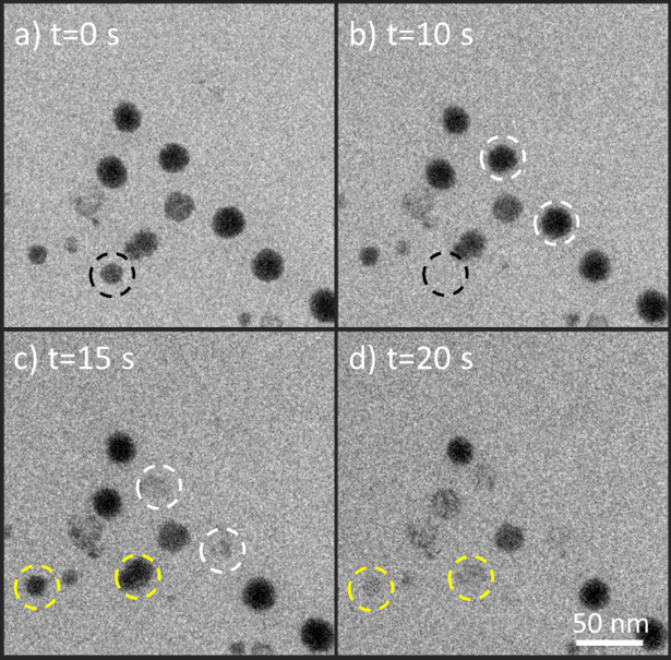
Figure 21: Dissolution of Au NPs under an electrochemical potentiostatic bias observed via in-situ EC-LTEM. Colored dotted circles mark the dissolution of various NPs at various stages.
We are actively involved in the ESTEEM consortium within the ESTEEM3 project (Enabling Science and Technology through European Electron Microscopy – https://www.esteem3.eu/) in the development of various state-of-the-art Transmission Electron Microscopy techniques (TEM) and materials characterisation. The Microscopy research group stays strongly connected with the activities within the Center for Electron Microscopy and Microanalysis (CEMM), mainly through the implementation of various electron microscopy analytical techniques and the possibility for the researchers to access research infrastructure for electron microscopy.